
Open for Business
The founding series closes. The platform opens. Here is what we built, who it is for, and how to engage with it. Nuno Edgar Nunes Fernandes Founder, Precision with Light

This is the fifth and final post in the Precision with Light founding series. If you are reading this without the previous four posts, the short version is: we built a physics-informed AI platform for photonic design — fiber optics, silicon photonics, quantum photonic processors — that answers the question every optical engineer asks but no existing tool can answer: given what I need the light to do, what geometry should I build? The long version is in Posts 1 through 4. This post is about what comes next.
What the Founding Series Actually Was
Four posts. Four months. One argument built in stages.
Post 1 established the existence proof: six research papers, each describing a different instance of the same abstract design problem, collectively making the case that a generative inverse design platform for photonics was not just possible but necessary.
Post 2 made the technical case for inverse design as a categorical capability shift — not a faster version of the same workflow, but a workflow that did not previously exist.
Post 3 situated the platform at the intersection of three converging forces: the data center bandwidth crisis driving co-packaged optics deployment at scale, the programmable photonic mesh enabling software-defined silicon photonic hardware, and the quantum photonic processor scaling from 8 to 20 modes and beyond.
Post 4 addressed the hardest question directly: why should you trust an AI-generated photonic design? The answer required being honest about where black-box machine learning fails in physical design contexts, and specific about how physics-informed neural networks with solver-verified outputs change that calculus.
Together they built a single argument: the photonics industry is at an inflection point where the design software layer has become the rate-limiting constraint, and physics-informed generative AI is the only credible architecture for removing that constraint without sacrificing the physical rigour that fabrication demands.
That argument is now complete. This post is about the platform it justifies.
The Architecture, Stated Simply
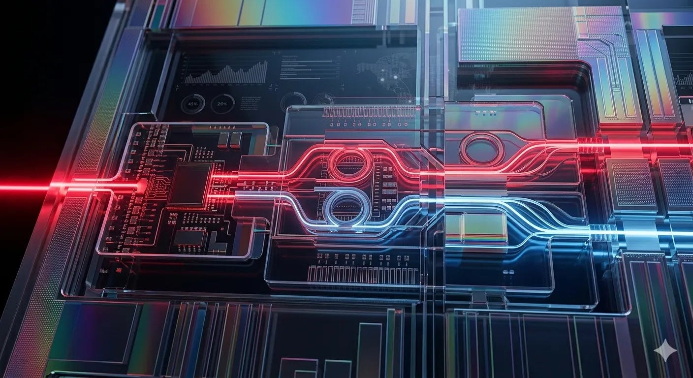
Precision with Light is a four-layer platform. Each layer has a specific job, and the layers are deliberately separated so that each can be improved independently without breaking the others.
Layer 1 — The Intent Layer translates what you want into what the physics allows. A natural language design brief — “I need a hollow-core fiber for gas sensing at 1550nm with less than 0.01 dB/m loss and an overlap factor above 0.95” — enters the DSR-CRAG (DSR-CRAG: A Double-Stream Corrective Retrieval-Augmented Generation Framework for Countless Intent Detection) system, which retrieves the relevant physical constraints from the database, checks the request against fabrication design rules, and produces a structured physics constraint document before any geometry is generated. The constraint check happens first. Always.
Layer 2 — The Generative Engine synthesises geometries from constraints. Physics-Informed Neural Networks have internalised Maxwell’s equations — they cannot produce an effective index above the core material’s refractive index, because doing so would increase the physics loss term during training. Conditional Wasserstein GANs explore the feasible design space and produce candidate geometries that satisfy the constraint document from Layer 1. The engine operates in milliseconds per candidate. A complete design exploration that would take weeks of FEM (Finite Element Method) simulation takes minutes.
Layer 3 — The Simulation Bridge verifies every AI-generated geometry against an independent solver before it leaves the platform. Lumerical FDTD and FDE (Finite Difference Eigenmode) for full three-dimensional device characterisation. COMSOL Multiphysics for fiber cross-section mode solving and thermal analysis. Tidy3D — Flexcompute’s cloud-native GPU-accelerated FDTD — as the preferred backend for silicon photonic components, accessible via API without local installation. Every design that reaches a user carries a solver-verified certificate: the simulated result matched the AI prediction within the specified fidelity threshold. If it did not, the platform flags the discrepancy and requests additional training data in that region of design space.
Layer 4 — The Fabrication Export converts verified designs into files that foundries and fabrication facilities can use directly. GDSII layouts for silicon photonics MPW runs at AIM Photonics, IMEC iSiPP50G, and GlobalFoundries GF Fotonix. STL meshes for two-photon polymerisation printing. Fiber draw tower specifications for specialty fiber manufacturers. OpenEPDA-compatible PDK ingestion — the standardised photonic PDK format developed through the JePPIX consortium — so that foundry design rule updates propagate automatically into the constraint database without manual re-entry.
The platform does not produce interesting geometries. It produces geometries that can be built, in specific materials, on specific process nodes, with specific fabrication tolerances, verified by independent simulation.

What the Platform Covers Today
The founding corpus defined the initial design families. The platform currently addresses:
Specialty fiber design — Large Mode Area fibers (comb-index, anti-resonant tube, step-index), hollow-core photonic crystal fibers (bandgap, anti-resonant, inhibited coupling), nonlinear PCF for four-wave mixing and supercontinuum generation, and the emerging family of sapphire PCF sensors for extreme-temperature applications covered in the Research & Technology track last week.
Silicon photonic integrated circuits — SOI waveguide design on AIM Photonics 300mm and IMEC iSiPP50G process nodes, ring modulator optimisation, directional couplers, grating couplers and edge couplers (including the adiabatic fiber-to-chip coupler architecture covered in the Research & Technology track two weeks ago), and wavelength-division multiplexing components.
Silicon nitride integrated photonics — Si₃N₄ waveguides, splitters, polarisation beam splitters, and mode multiplexers for the quantum photonic processor platforms built by companies like QuiX Quantum and LIGENTEC, where two-photon absorption in silicon makes Si₃N₄ the mandatory material choice.
Programmable photonic meshes — Non-uniform hexagonal waveguide mesh topology optimisation for Field Programmable Photonic Gate Array architectures, including defect cell placement for Vernier-extended free spectral range. This vertical was mainly inspired by the work of José Capmany Francoy and team at the Universitat Politecnica de Valencia, Spain.
Photonic tensor processors — The neuromorphic computing domain covered in the Research & Technology track’s first post: incoherent crossbar architecture design, electro-absorption modulator geometry, and microcomb source specification for AI inference hardware — the design family that will define the next generation of optical AI accelerators.
Who the Platform Is For
Three distinct audiences. Three different engagement models.
Academic research groups working on photonic design, fiber fabrication, silicon photonic integration, or quantum photonic processors. The platform accelerates the exploration phase of a research project — generating families of candidate geometries across a parameter space that would take months to cover by manual FEM simulation, allowing researchers to focus expert time on the most promising candidates. Academic access is available at no cost for non-commercial research use, subject to attribution. If your group is designing PCF structures, silicon photonic PICs, or quantum photonic processor layouts and you are spending weeks on parameter sweeps that could be done in hours, reach out.
Industrial R&D teams at photonics companies, optical system integrators, and semiconductor manufacturers whose product roadmaps require photonic integrated circuit design faster than current manual workflows allow. The Lumentum supply constraints, the Credo DustPhotonics acquisition, the NVIDIA laser investment — all of these are expressions of an industry that is scaling faster than its design tooling. If your team is designing fiber lasers, CPO transceivers, silicon photonic switches, or photonic AI accelerators, the platform is designed to integrate into your existing design flow as an upstream generative layer above your simulation tools, not as a replacement for them.
Research and technology partners interested in co-developing specific design modules, integrating the platform’s outputs with their fabrication processes, or building joint academic programmes around the platform’s capabilities.
The Partnership Landscape
Three specific partnership conversations are already open or actively being developed.
Flexcompute / Tidy3D — the Simulation Bridge integration is already fully specified. Tidy3D becomes the cloud-native FDTD verification backend for silicon photonic designs, accessible via API without local Lumerical or COMSOL installation. For academic users and startups without expensive simulation tool licenses, this is the path to a fully functional end-to-end design and verification workflow. The Tidy3D adapter specification has been written and is ready for implementation the moment the API integration is formalised.
The JePPIX / European MPW ecosystem — JePPIX is the Multi-Project Wafer consortium that provides access to InP and silicon photonic foundry runs for European academic and industrial users. The OpenEPDA standardised PDK format, developed through JePPIX partners including TU Eindhoven, is the target input format for the platform’s fabrication constraint database. A partnership with JePPIX-affiliated foundries would give platform users a direct path from AI-generated, solver-verified design to physical chip — the complete pipeline from natural language intent to fabricated device.
Opdo.ai — the AI-native optical component design company working in volumetric fabrication for optical coatings, free-form lenses, and metasurfaces. The complementarity is specific: Precision with Light handles upstream electromagnetic design and simulation verification for the photonic waveguide and fiber layer; Opdo.ai handles downstream volumetric manufacturing for the free-form optical layer. The integration point is the platform’s STL export, which feeds directly into Opdo.ai’s manufacturing intake. The joint value proposition — software-defined photonic design from physical specification to fabrication-ready file, spanning both guided-wave photonics and free-form optics — addresses a capability gap that neither platform covers alone.
What Comes Next
The founding series is complete. The two-track weekly publication — Research & Technology on Tuesdays, Business of Photonics on Thursdays — is now in its regular cadence and will continue independently of the platform’s development milestones.
Three major deliverables are in active preparation:
The arXiv preprint — a technical paper on the DSR-CRAG architecture: Dual-State Corrective Retrieval-Augmented Generation for Physics-Constrained Photonic Design Synthesis. The founding corpus across all five posts provides the citation backbone. The multi-level PINN framework, the surrogate modelling methodology, and the experimental validation cases across fiber, silicon photonic, and quantum photonic design families are all documented. The preprint will be submitted to arXiv under physics.optics and cs.AI, and announced in this publication when it goes live.
The Pydantic schema and FastAPI endpoint release — a complete, publicly documented API specification for all platform design families, with Pydantic v2 data contracts, OpenAPI schema export, and endpoint specifications for the generative design, simulation verification, and fabrication export workflows. This is the technical artefact that allows integration partners and academic users to build on top of the platform programmatically.
The MPW batch endpoint — Multi-Project Wafer batch design submission, allowing multiple independent PIC designs to be packed onto a shared reticle area with automated DRC sign-off and direct submission to AIM Photonics and IMEC MPW run schedules. This is the capability that makes the platform directly useful for the academic research groups and startups that cannot afford dedicated wafer runs but need physical silicon to validate their designs.
The One Sentence Version
The photonics industry is producing record revenues, record acquisition prices for PIC design IP, and record supply constraints — all simultaneously, as covered in this publication’s Business of Photonics track over the past two months. The design software layer that makes those chips faster to design, more reliably validated, and more directly connected to fabrication is the gap the platform fills.
If that sentence describes a problem your organisation is navigating, reach out.
The founding series is complete. The Research & Technology and Business of Photonics tracks continue every week. The platform is open.
Subscribe below if you are not already a subscriber. Share this post if someone in your network should be reading it.
Nuno Edgar Nunes Fernandes Founder, Precision with Light precisionwithlight.substack.com · GitHub