
Light Does the Maths: Inside the First Production-Grade Photonic Tensor Processor
Precsion with Light Research & Technology #2. Co-written, edited and curated by Nuno Edgar Nunes Fernandes

A Nature Communications paper from Heidelberg and Enlightra just moved photonic neuromorphic computing from demonstration to deployment-ready hardware. Here is what it actually achieved — and what it means for Photonics Research.
Why Tensor Operations Are the Bottleneck
Every time a large language model generates a token, every time a computer vision system identifies an object, every time a scientific simulation runs a forward pass — the dominant computational operation is the same: a matrix-vector multiplication. Multiply a weight matrix by an input vector, accumulate the results, apply a nonlinearity, repeat hundreds of times per layer and thousands of layers deep.
At the scale of modern AI inference — GPT-class models, vision transformers, protein folding networks — this amounts to hundreds of billions to trillions of multiply-accumulate (MAC) operations per inference pass. The silicon doing this work is fast, but it is not free. Each MAC operation charges and discharges capacitors, moves electrons across resistive connections, generates heat, and consumes power. At data center scale, the aggregate energy cost of this is one of the defining infrastructure challenges of the next decade.
The photonic computing community has argued for years that there is a better way: perform the linear algebra in the optical domain, where signals travel at the speed of light, without resistive loss, without capacitive charging, and without electrical crosstalk. The argument is physically sound. The implementation challenge has been formidable.
A paper published April 9 2026 in Nature Communications, from a team at the Kirchhoff-Institute for Physics at the University of Heidelberg together with Enlightra — a Swiss microcomb startup — represents the most complete answer to that implementation challenge demonstrated to date. It is worth reading carefully.
What Was Actually Built
The paper presents a photonic tensor processor (PTP) that performs deep neural network inference using an all-optical crossbar architecture, packaged into a standard 19-inch rack unit with a high-speed electronic interface to PyTorch.
Let us be precise about what each of those elements means.
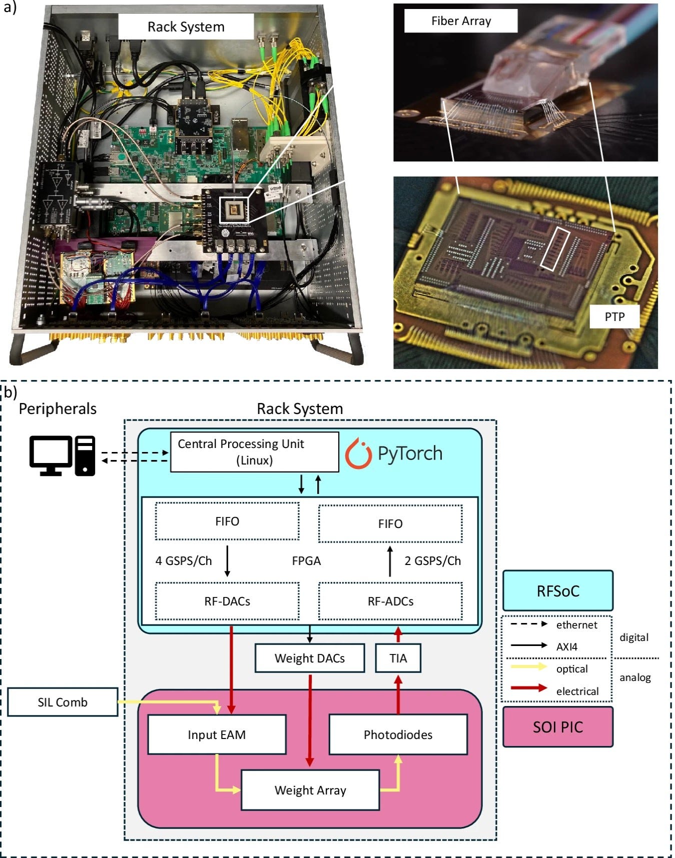
The crossbar: A 9×3 incoherent optical crossbar — nine inputs, three outputs. At each input, an electro-absorption modulator (EAM) encodes a vector element by modulating the intensity of an incoming light beam. At each intersection of the crossbar, a second EAM sets a weight by controlling how much of that intensity passes through. The modulated intensities from all nine inputs propagate to the three outputs, where on-chip SiGe photodiodes sum them through optical power accumulation — literally adding intensities — and convert the result to an electrical current. This is a parallel, all-optical matrix-vector multiplication.
The word “incoherent” is important. Most earlier photonic computing demonstrations used coherent architectures — Mach-Zehnder interferometer meshes where phase relationships between beams encode the computation. Coherent systems offer high precision but require tight phase control across the entire chip, which is difficult to maintain at scale. The Heidelberg group’s incoherent approach uses intensity, not phase — simpler to calibrate, more robust to fabrication variation, and more compatible with the kind of weighted optical power accumulation that maps naturally to neural network multiply-accumulate operations.
The light source: A self-injection-locked microcomb based on a high-Q Si₃N₄ microresonator, supplied by Enlightra. A microcomb generates a comb of equally spaced optical frequencies from a single pump laser — in this case with a 485 GHz free spectral range, producing multiple wavelength carriers simultaneously. Each wavelength channel carries one input of the nine-input vector in parallel. This wavelength-division multiplexing of the computation is one of the most elegant aspects of the architecture: rather than time-multiplexing the inputs sequentially, all nine inputs are processed simultaneously on different wavelength channels, and the photodiodes integrate across all wavelengths naturally.
The use of a microcomb as the source — rather than nine individually stabilised lasers — is not merely an engineering convenience. It is what makes the system practically deployable. Nine separate tunable lasers, each requiring active wavelength locking, would introduce a calibration and reliability burden that would dwarf the computational advantage. The SIL microcomb solves this in a single, packaged, low-noise source.
The silicon photonics platform: The chip is fabricated on imec’s iSiPP50G process — the same European silicon photonics foundry platform that appears in the co-packaged optics and programmable photonics discussions throughout this series. This is not an academic custom process. iSiPP50G is a production-accessible, multi-project-wafer platform with established design rules, a PDK, and a known yield profile. The fact that a photonic AI accelerator demonstrating state-of-the-art DNN inference was built on this platform is a strong signal about where the field is heading: toward foundry-compatible, replicable photonic computing hardware.
The electronic interface: A ZCU216 RFSoC FPGA running at 4 GS/s for EAM modulation and 2 GS/s for readout, connected to a Jupyter server via Ethernet, with direct PyTorch integration. The computational model is: the GPU or CPU runs the network up to a linear layer, offloads the matrix-vector multiplication to the photonic processor, receives the result, applies the nonlinearity digitally, and continues. The handoff is seamless from PyTorch’s perspective — the PTP appears as a hardware backend, not unlike how a GPU appears as a CUDA device.
Keep reading with a 7-day free trial
Subscribe to Precision with Light to keep reading this post and get 7 days of free access to the full post archives.